Despite being an aged piece of electrical technology a flex PCB still holds value in this present era even when pitted against its contemporaries. Over time it has proven itself as a huge game-changer in the world of electronic manufacturing where it offers unequaled flexibility and versatility.
In this article we’ll be exploring what a flex PCB is and also discuss the intricate techniques and processes utilized in manufacturing these technological marvels by flex PCB manufacturers.
Flex PCBs: an overview
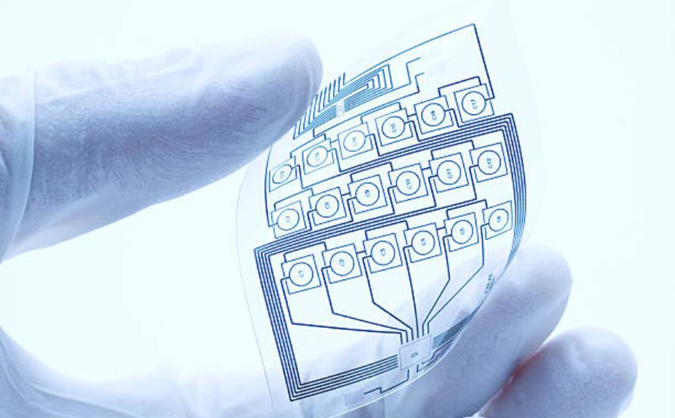
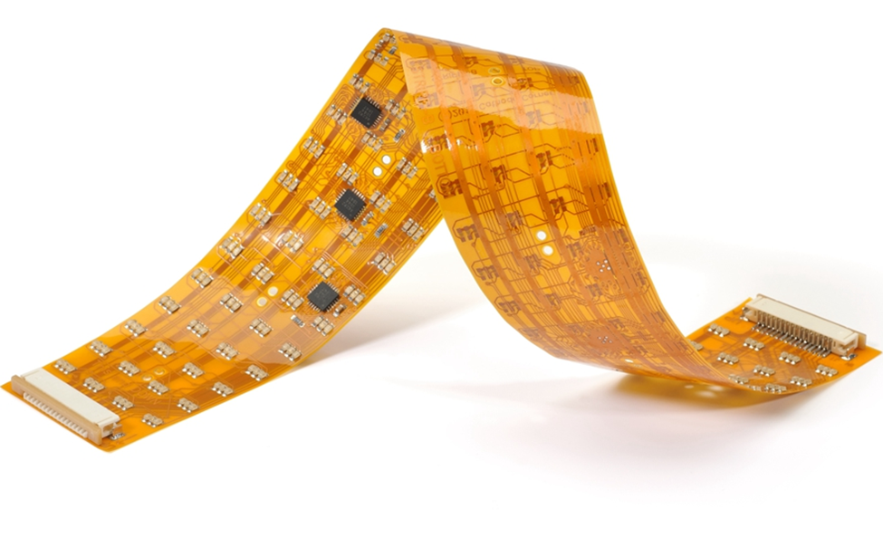
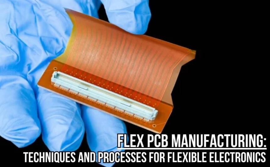
Before we explore the techniques and processes used in manufacturing this PCB let’s familiarize ourselves with what is a flexible printed circuit board. A flex PCB board is a type of circuit board that is defined by its thin yet tensile properties. This type of PCB tends to see widespread use in electrical industries since it is easy to bend and fold into electrical configurations without causing damage to the setup.
Devices that utilize this type of printed circuit board are the likes of televisions fridges clocks and certain varieties of phones. Another property to take note of is that flex printed circuit boards are cheaper on purchase and in the long run compared to regular PCBs again due to their tensile nature making them deceptively durable.
The techniques and processes of fabricating Flex PCBs
The tensile flexible printed circuit board requires the use of different techniques and processes to ensure that it will exhibit the key traits of its type of circuit board. In this section we’ll be exploring what techniques and processes are used in flex PCB fabrication.
1. Creating the concept design
The design serves as the foundation of how a flex PCB will be made and how the layout should look like. The design that you’ll create also indicates which materials are needed what components need to be present and many more. Creating a design that will act as a reference material is crucial to creating a flexible printed circuit board that matches your intent.

2. Preparation of the base material
Once the design is completed the next step in flex PCB fabricating a flexible printed circuit board is to prepare the production panels which are cleaned with the use of a special cleaning agent before a light-resistant film is added to them. The flex PCB boards usually use a polyimide-base material as their base material but the selection of the base material is determined by the components present the speed of manufacturing the boards etc.
The base material is given one or two layers of copper which are deposited (or rolled annealed) on the surface of flex PCB base material. The copper is etched and given patterns to form traces and reveal the components inside the board. Upon finishing the etching process the base PCB is prepared and is ready to proceed to the next step.
3. Exposing the circuit patterns
Once the flex PCB is properly prepared the next step is to expose the circuit patterns through the application of light-resistant coating panels. These panels are then exposed to ultraviolet light where the intent here is to expose the copper traces that form link the internal components in the flexible circuit board.
You will also need the stencil for this step so you can create a masking layer for etching the copper traces.
4. Etching the flex PCB
The next step of the process is to etch the printed circuit board by removing the excess copper. This is done by soaking the board in an etchant liquid that dissolves the unwanted copper which is conducted inside a plating tank. This process will expose the pads and areas where the components of the flex PCB board will be soldered.The goal of this step is to fill in pads and traces on the circuit board to expel unwanted or excess materials.
Take note that this process requires the use of sacrificial materials that will protect the components from damage during the etching process.
5. Drilling holes
After you finish etching the flex PCB board you’ll need to start drilling holes in the circuit board to form pathways where you can insert and solder the components that will be added soon. For double-layer and multilayer flex PCBs the holes are used to connect the copper wires in different layers. The holes are drilled from the back section of the board. This process is facilitated by high-speed machines that can precisely poke small holes into the circuit boards which will form a network of holes that form a pattern on the board.

6. Addition of copper plating
The next step in flex PCB fabrication is the application of copper plating on the drilled boards. The goal of this step is to add copper in the holes and then the copper traces in different layers can be connected. The plating chemical is kept in place by gravity ensuring that they are spread evenly on the PCB.
The addition of copper plating also ensures that the conductors and pads have enough copper thickness.
7. Application of cover layers and stiffeners
Before lamination you will need to add coverlay panels on the flex PCBs. You will need to sandwich the critical component between two coverlay sheets to protect them from damage. You’ll need to drill holes through these panels and apply permanent glue to keep the panels intact and prevent board damage.
After adding coverlay sheets the next phase involves the addition of stiffeners before the PCBs are tested and given a final inspection. The stiffening panels can be placed on one or both sides of the PCB and act as a barrier between the solderable surface and insulation layers; but also as an additional measure of protection as it contributes to the flex PCB’s durability.
8. Performance tests and final inspections
The final steps in the process of flex PCB fabrication are the performance tests and final inspections. These steps are intended to ensure whether the flexible printed circuit boards are working as planned according to the design but also to check whether the boards have some physical defects. E-testing for open and short circuits and AOI checking is the most usual methods.
If the tests and inspections reveal that the boards have underlying issues they are either repaired or remanufactured by flex PCB manufacturers. But if the boards don’t show any signs of errors or defects they are prepared for packaging and are shipped to the client that purchased them.
An intricate process for an aged yet very effective circuit board
Flex PCB manufacturing is a complex process that has managed to withstand the tests of time which shows that they are a cornerstone in the world of electronics. Even though flex PCBs are showing their age the techniques and the processes that flex PCB suppliers use show that these flexible boards continue to stand at the forefront of innovation.
As we gaze into the upcoming years it is clear that flex PCBs will continue to play an important role in shaping and defining the future generations of flexible electronics.


